DDS Function Generator with STM32F405
DDS Function Generator with STM32F405
Article under development. Some sections are not complete.
Thank you for your patience.

✔️ Introduction
This project is an extension of the DDS Discovery Board Shield (Link) done for the Embedded Systems class of 2024.
Note: DDS stands for Direct Digital Synthesizer and you can check this link for more details.
The DDS Discovery Board Shield doesn't have a microcontroller and it needs an external +/- 13V power supply for the Op Amps. It is a shield for the STM32F407 Discovery Board that allows the user to experiment and thinker with DDS algorithms.
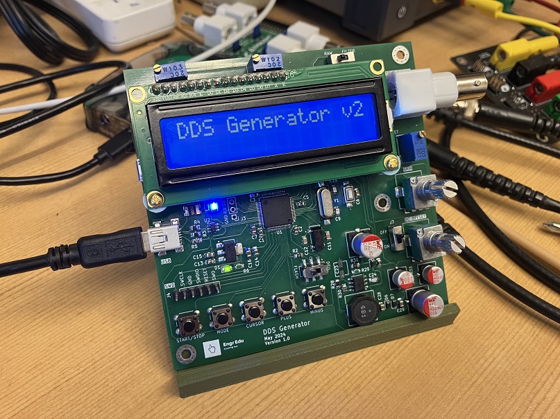
This extension aims to include its own microcontroller (an STM32F405) and supply power to the entire system out of a 5V USB cable. That means that it has the circuitry to convert 5V to +/- 13V.
✔️ Reference Projects
The original motivation for this project is based on the DDS Function Generator from Amazon (Link).
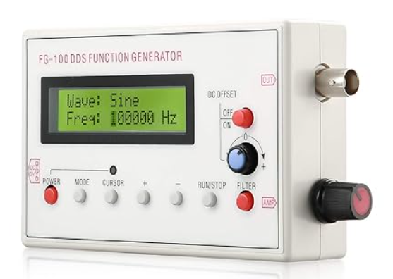
There is a blogpost (Link) that goes over some details of this DDS device, in particular the different functional parts of the system.
There are also plenty of YouTube videos showing the pros and cons of this DDS Function Generator. However, you can't find many resources showing how to build one from scratch.
I will be replicating the majority of these functional parts and providing additional information about the circuits and code.
This new board will also have the ability to be controlled by UART, offering an additional feature to the existing system.
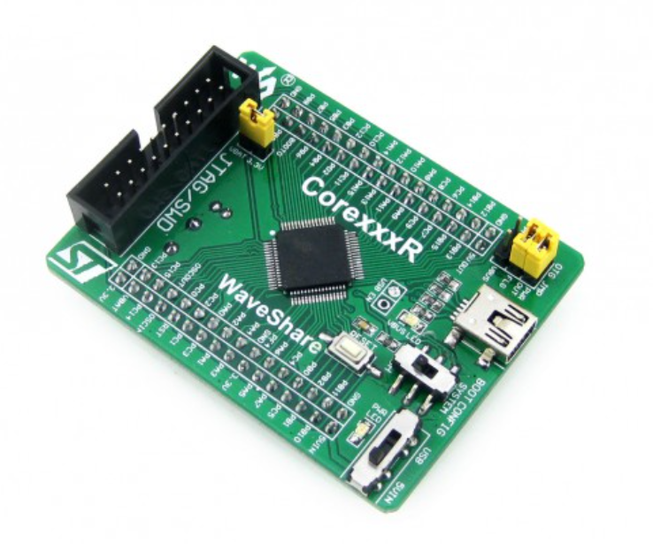
Instead of using the ATMega48, I will be using the STM32F405. For that, I will be reusing the designs from Waveshare Core405, STM32F4 Core Board (Link) reference schematics.
✔️ Design Stage (Block Diagrams)
Let's start with showing the block diagram with all the functional parts of the new DDS Function Generator.
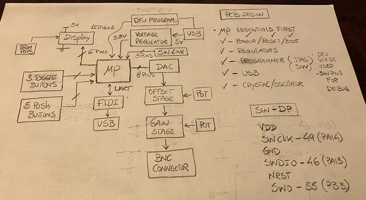
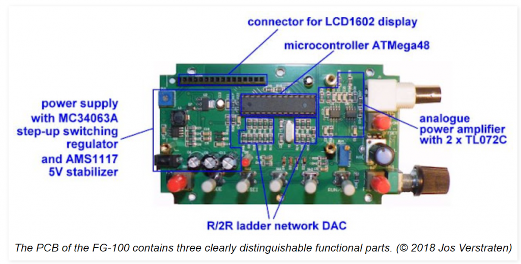
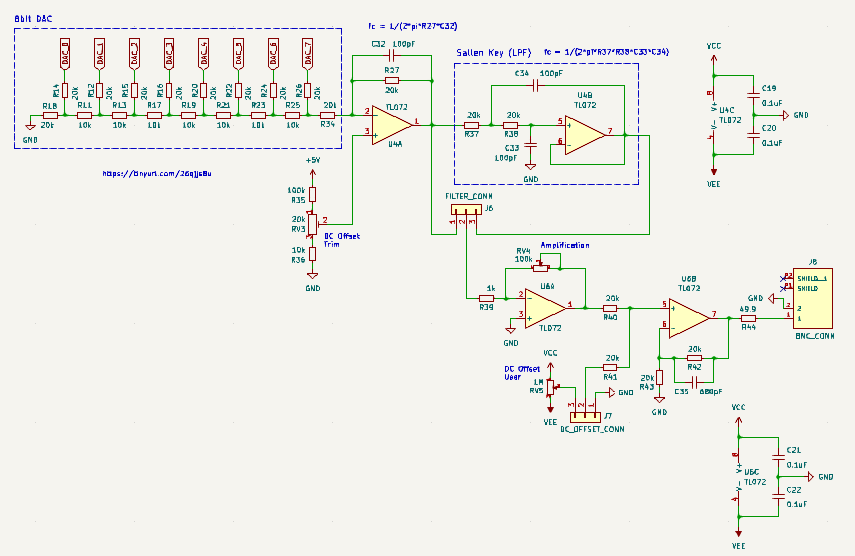
Instead of using an off-the-shelf DAC, I will be building one from scratch, similar to the FG-100 DDS board. I will include an offset correction circuit, gain stage and additional filtering.
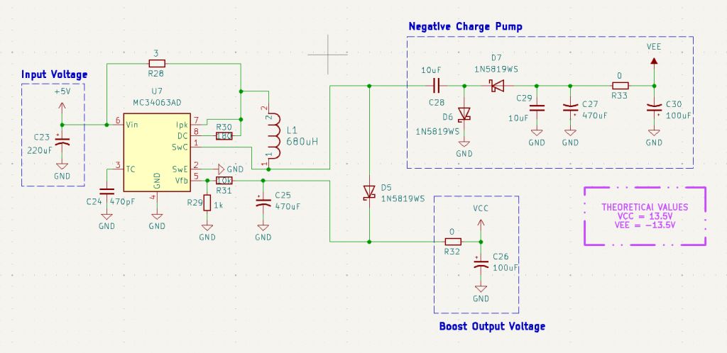
To get +/- 13V from the USB 5V cable, I will be using a boost converter with a negative charge pump.
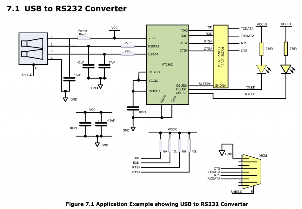
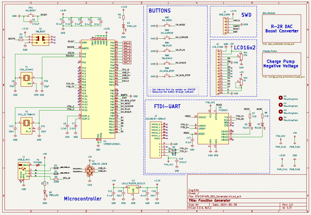
For the USB to RS232 circuit, I will be using the FT230XS-U from FTDI and using their datasheet application example as a reference design.
For the microprocessor and respective voltage regulator, oscillator and programming pins, I am reusing the schematics from Waveshare Core405 board (Link).
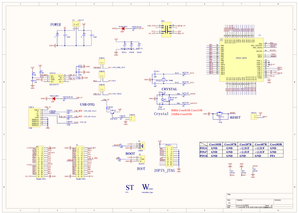
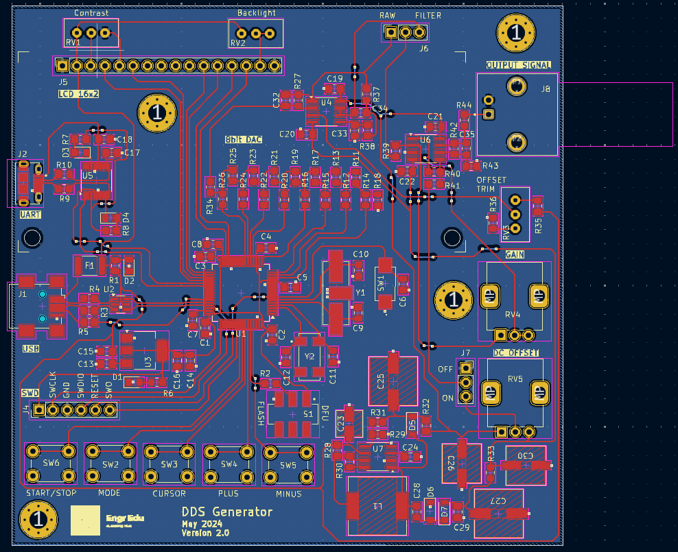
For the rest of the components, buttons and LCD, the PCB design schematic should be sufficient to understand how the integration of those elements were done with the board.
✔️ Prototype Stage
All tests were conducted using an STM32F407 Discovery Board. However, the code for the STM32F405 will be exactly the same. The pinout will be changed accordingly during the PCB Design stage.
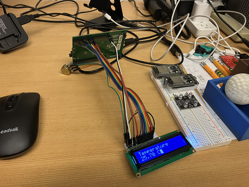
LCD Test
The LCD was the first element to be tested. I will be using the common 16x2 serial LCD screen used in several online Arduino projects.
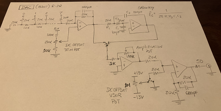
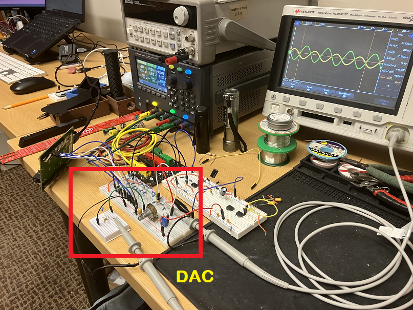
R-2R DAC Test
For the DAC, I designed an 8 bit R-2R ladder circuit.
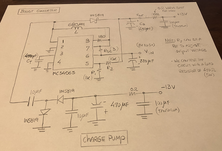
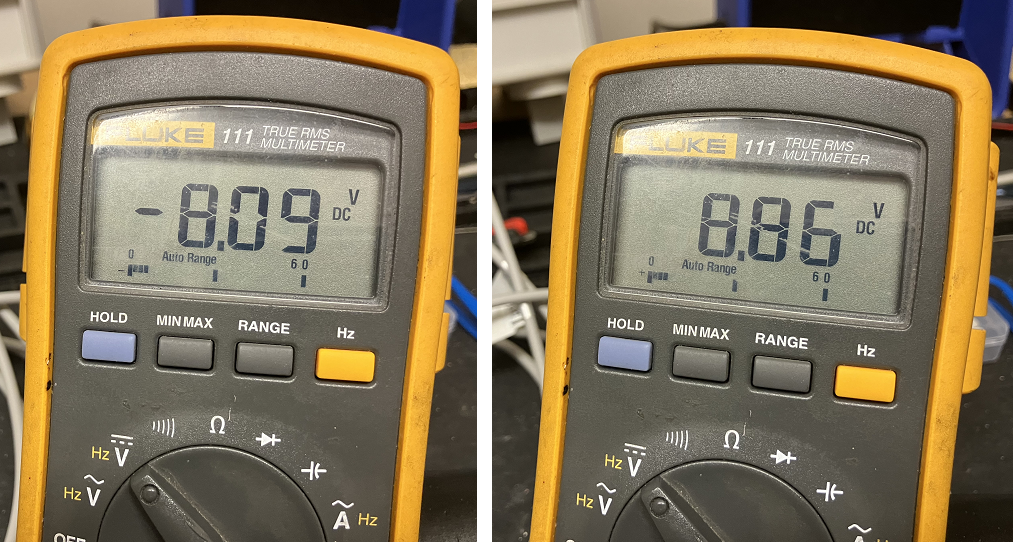
Boost Converter and Charge Pump
For the boost converter, I used this wonderful video to help with the circuit analysis and components selection. After testing it with no load, the boost converter provides de +13V to the circuit. For the charge pump, you can get a general idea on how it works from this link. The charge pump receives +13V from the boost converter and converts it to -13V. The circuit was then incorporated with the DAC.
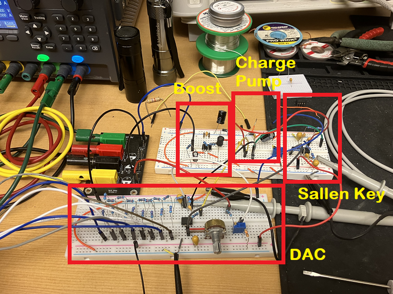
With a load in front the boost converter and charge pump, the +/- output voltages dropped to about +/- 8V. Unfortunately, I couldn't pinpoint the problem on the breadboard, however, this stage works at +/- 13V as shown in "Testing Stage" section.
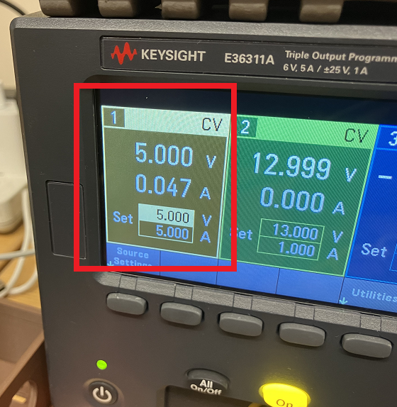
The overall current consumption of the system is around 47mA.
✔️ Assemble Stage
The boards were manufactured by PCBWay.
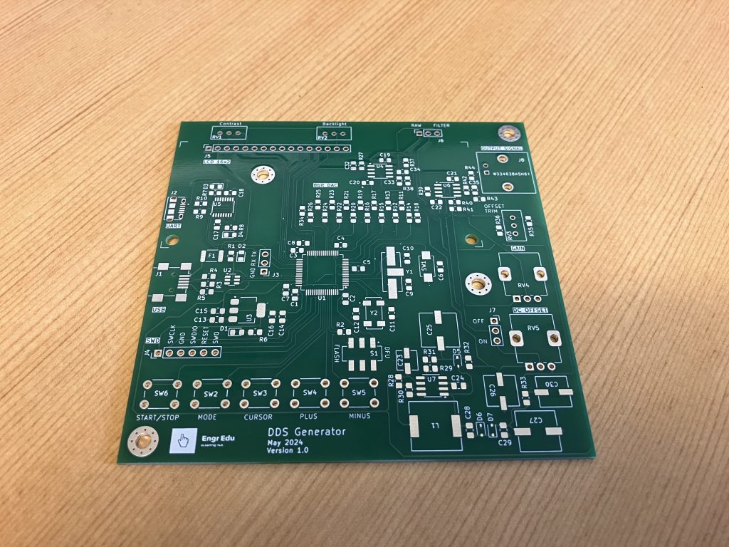
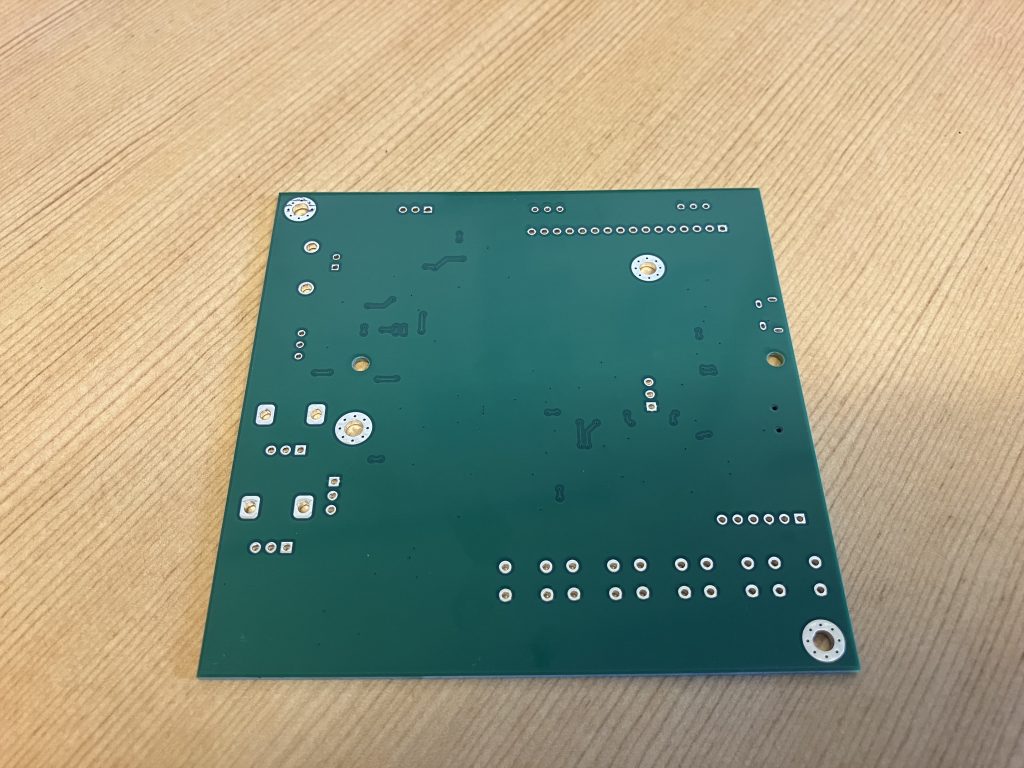
Assembled in house.
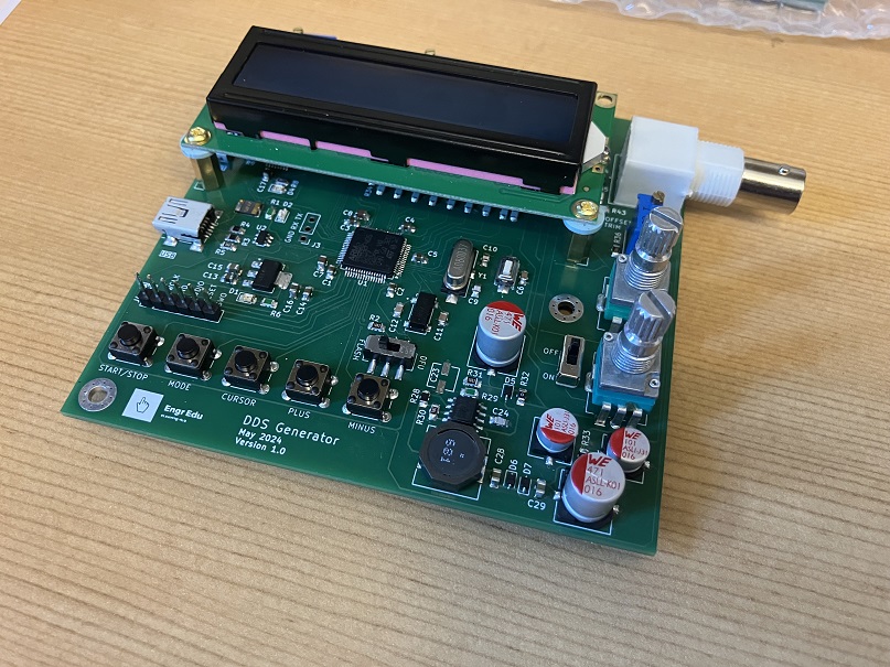
Note: I made a mistake on the original board on the RX and TX connections that needed to be swapped. All files on the GitHub repository, schematics and layouts shown on this article have that mistake corrected.
✔️ Testing Stage
Due to the complexity of this board, the tests were done in a incremental way to make sure that the components were being soldering correctly and the board was operating has expected.
For the testing phase, we will be using the following equipment:
- Oscilloscope from Digilent, Analog Discovery 2
- DDS STM32F405 Function Generator
- UART interface: Realterm
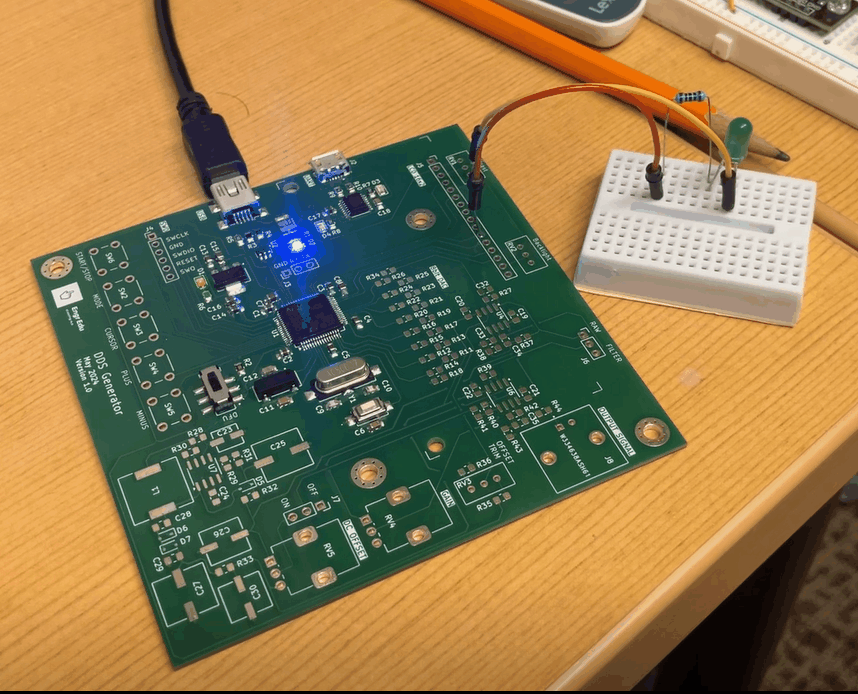
Blink LED Test
The first modules to be soldered were the USB connectors and respective electronics, voltage regulator and microprocessor. The pins used for the LCD were used to blink an LED.
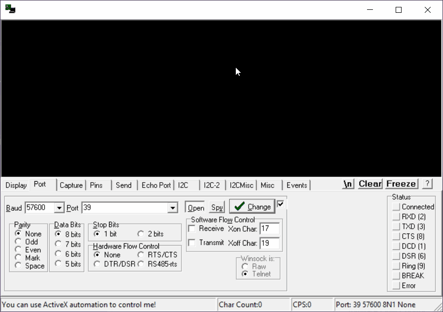
UART Test
A simple test of a UART loopback.
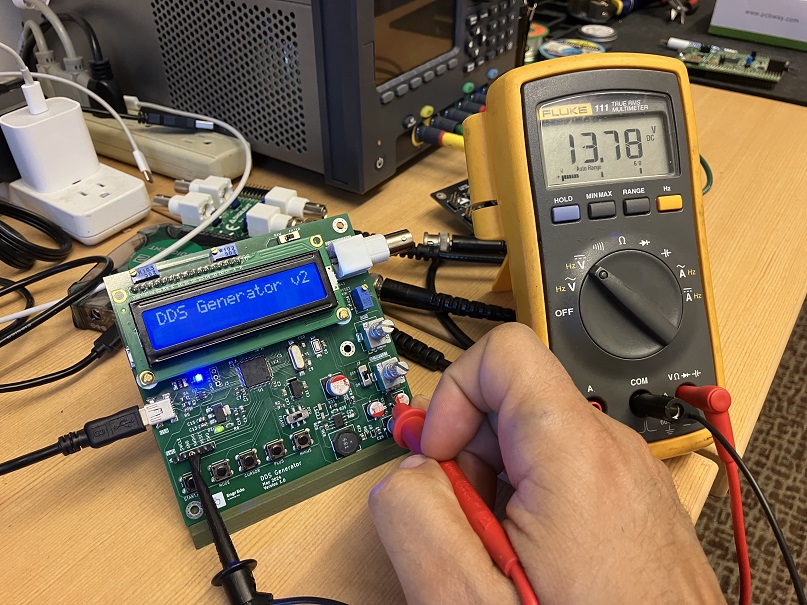
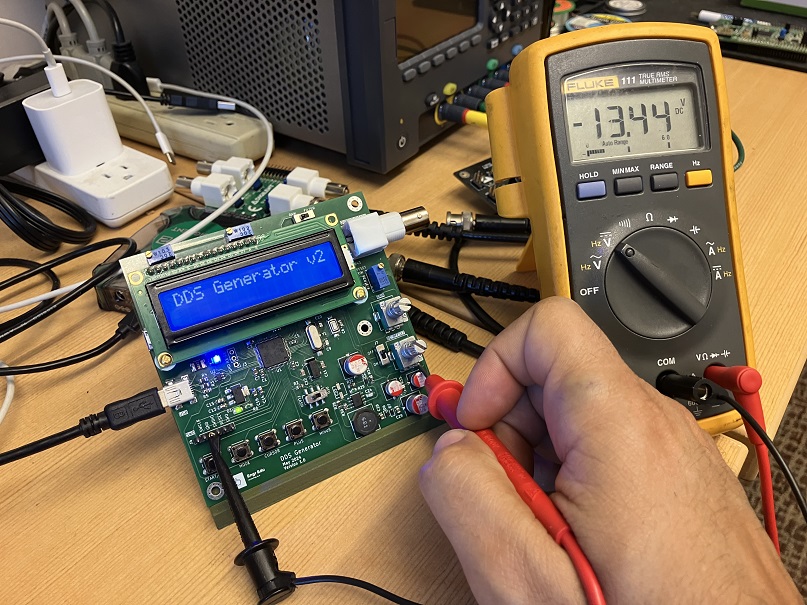
Op Amp Supply Rails
DAC Test
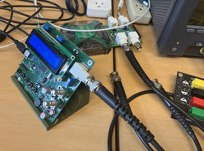
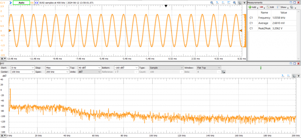
Sine waveform test and respective FFT.
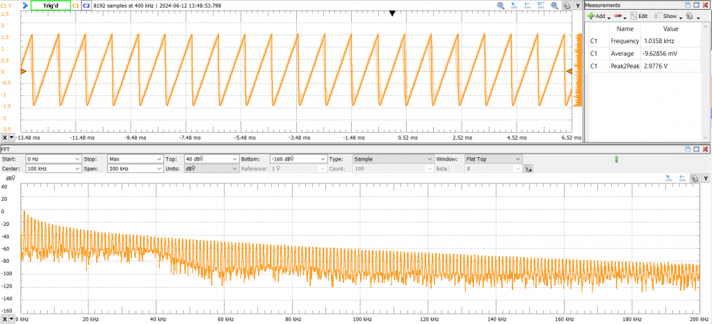
Sawtooth waveform test and respective FFT.
🔧 Performance Test
Soon...
🔧 GitHub Repository
✔️ References
- [Ref 1] “FG-100 Function Generator Tested”, Website [Article]
- [Ref 2] “Core405R, STM32F4 Core Board”, Website [Article]
- [Ref 3] “Building a Boost Converter From a Dinosaur”, The Offset Volt YouTube Channel [Video]
- [Ref 4] “Let's build a voltage multiplier”, Ben Eater YouTube Channel [Video]
Sponsor