Logisim Evolution FPGA Board Editor
Part 3: Logisim Evolution FPGA Board Editor
The Logisim Evolution version used in these articles supports Xilinx or Altera boards only.
The set of directions described below can be used for any Xilinx or Altera board as long as Vivado (for Xilinx) or Quartus (for Altera) supports synthesis for those boards.
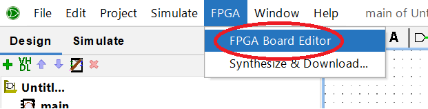
FPGA Board Editor
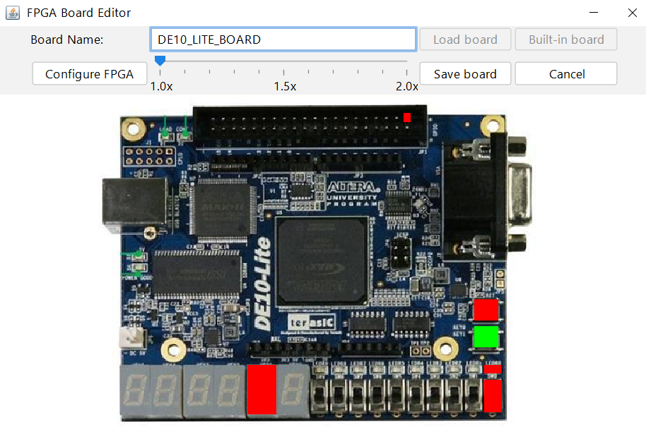
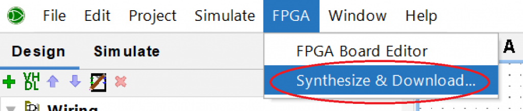
Go to the FPGA menu and select "FPGA Board Editor".
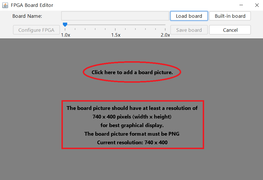
The first step is to get a picture of the board that you want to include in Logisim Evolution. The main requirement is that the picture should be 720x400 pixels (width x height) and saved as a PNG.
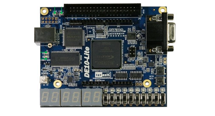
Example below for the DE10-Lite board. You can "Save image as..." this picture and use it a long the steps.
Next, click to add the board picture to the board editor.
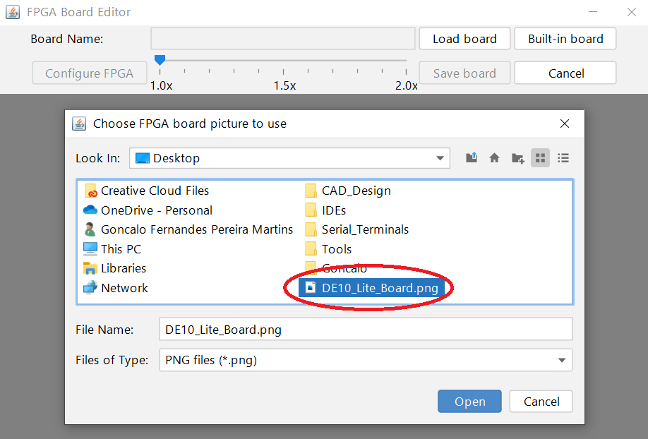
Give a descriptive name and press "Configure FPGA".
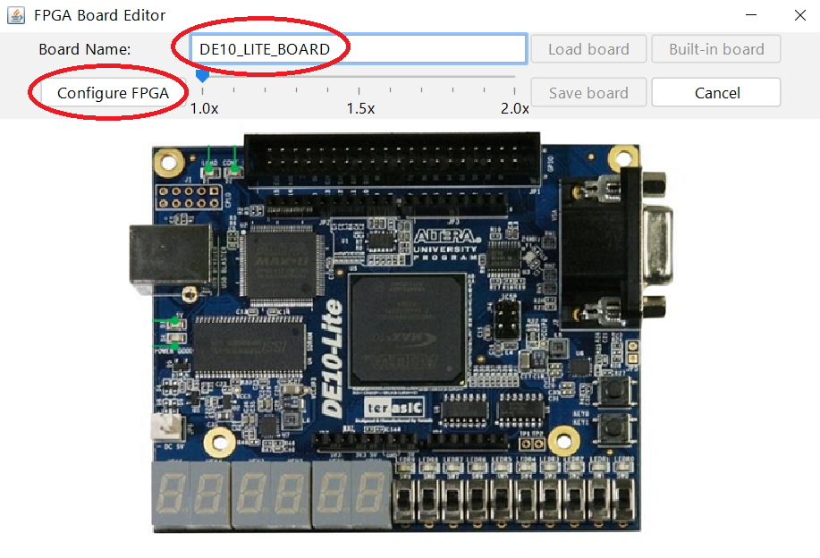
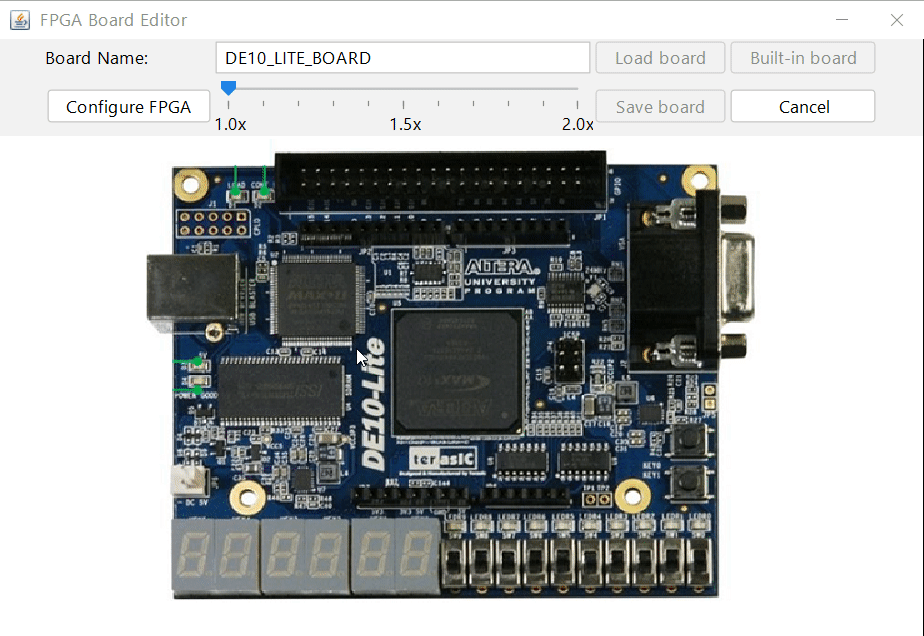
Configure FPGA
Second step, we need to configure the FPGA clock frequency and clock pin location, FPGA vendor, family, part, package, and speed grade.
You can find that information by looking at the development board manual or by using Vivado or Quartus software to help creating a project for that specific board and get the desired information from the created project specs.
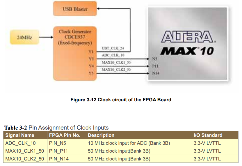
For the DE10-Lite board clock information, we can use the DE10-Lite manual. On page 24 we can find that the clock frequency is 50 MHz on pin P11 and a 3.3-V LVTTL I/O standard .
The DE10-Lite board has the MAX 10 10M50DAF484C7G chipset (Link). To understand what this number means, we can use the Intel® MAX® 10 FPGA Device Overview document. Figure 1 on page 5 can help getting the rest of the information.
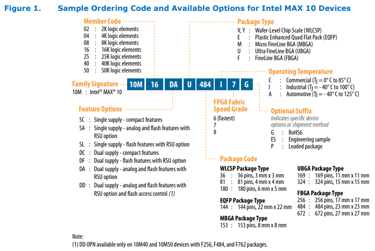
- FPGA Vendor: Altera
- FPGA Family: MAX 10
- FPGA Part: 10M50DAF484C7G
- FPGA Package: FBGA 484
- FPGA Speed Grade: 7
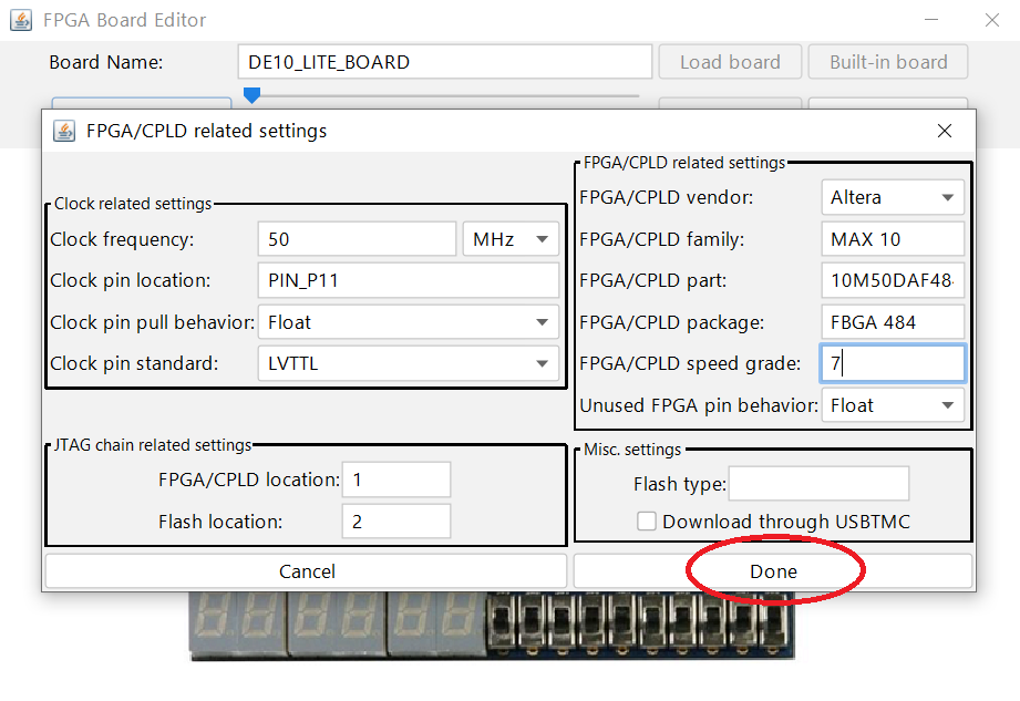
Press "Done".
Configure Pinouts
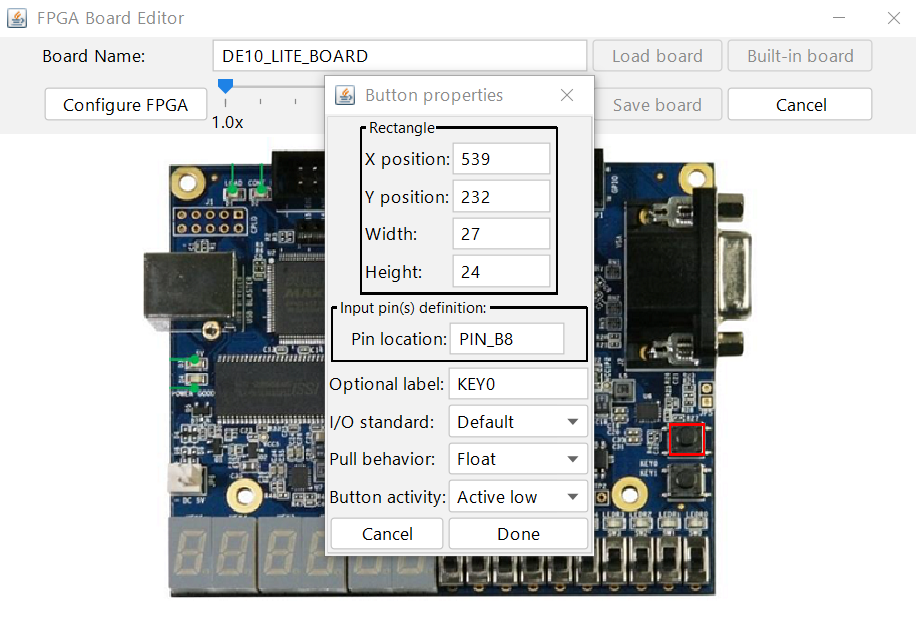
Third step, is to configure the pinouts. This is the tedious part of this all process. I recommend a lot of patience but it will pay off at the end.
Start by designing a square around the component (e.g. 7 seg display), or input or output pins, or buttons, or switches that you want to configure.
Select the type of I/O resource. In this particular case, it is a button.
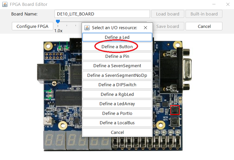
Fill the information for that I/O according to the specs of that pinout.
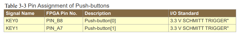
- For the rectangle specs, don't worry too much about it. We can change that later by editing the file (much easier than using the board editor).
- For the pin location, I/O standard and button activity, you can find that information on page 25 of the DE10-Lite manual.
Press "Save board" and save the file in a place where you know the file is.
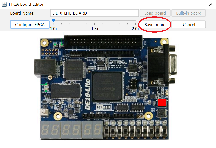
If you open the saved file, you can see that the information was saved in XML format.
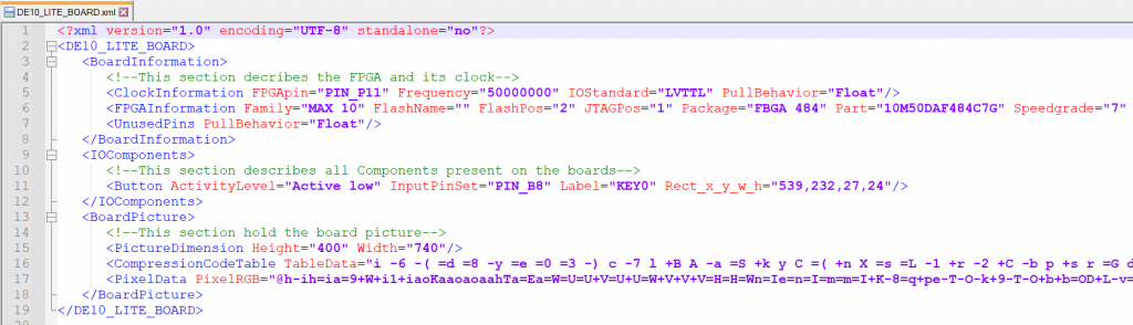
You can keep editing the board using Logisim Board Editor, however it does get frustrating when you need to edit a lot of pins that are pretty much the same.
We can accelerate this process by finding a good combination between editing the file and use the board editor.
Editing the XML Board File
What I recommend doing first, is to define ate least one pinout of each type using the board editor. With this we can get an idea on how the parameters are written on the XML file for that type of pinout. The size and position of the rectangle can be tweaked later on the XML file.
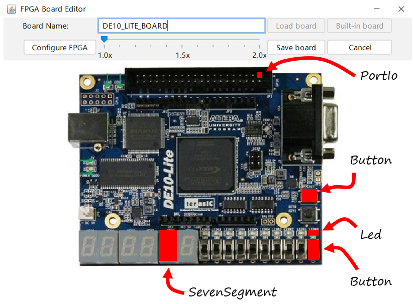
Remember to use the manual to get the pinout information. In this case you can find that information on
- page 25 for the key buttons
- page 26 for the switch buttons
- page 27 for the LEDs
- page 28 and 29 for the seven segment displays
- page 30 for the PortIo
Open the XML file and pay attention on how the information was written for the pinouts that were just added on the board editor.
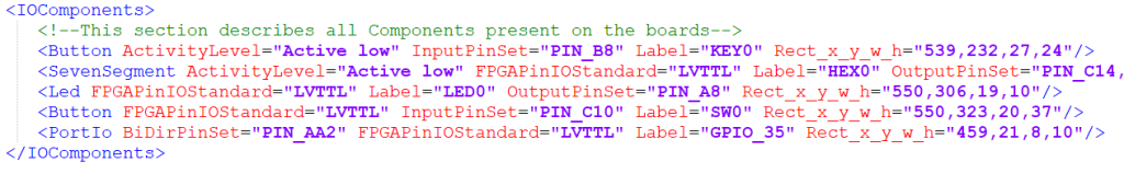
If you want to add the other components, copy the respective line and change the pin location, label, and the size and position of the red rectangle.
For example, add the following line to add "KEY1" into the board. The rectangle size (w and h) is the same as "KEY 0". X position is the same, and Y position gets shifted down until the rectangle is at the desired place.

Remember, it is a patience game. You repeat this process for the rest of the pinouts.
Boards XML Files
DE10-Lite Board Logisim Evolution XML File
Zybo z7-10 Logisim Evolution XML File (good clock pinout)
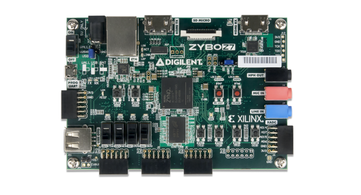
Note: Logisim Evolution comes with a Zybo z7-10 target board by default. Unfortunately, the template has the clock pinout in the wrong location - PIN_L16. The XML file above, as the clock pinout fixed - PIN_K17 (page 16 of the Zybo Z7 Board Reference Manual).
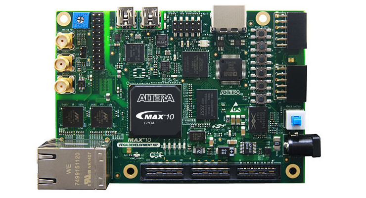
MAX10 Development Kit XML File
Add XML to External FGPA Board List
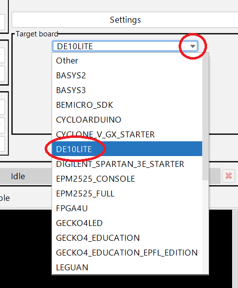
The last step, is to add the board to the list of target boards under the "Synthesize and Download" menu.
Go to "Settings"
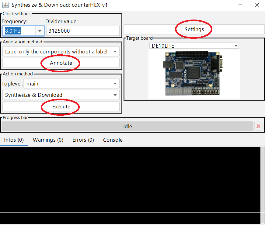
Press "Add a board" and select the XML file that you have been editing.
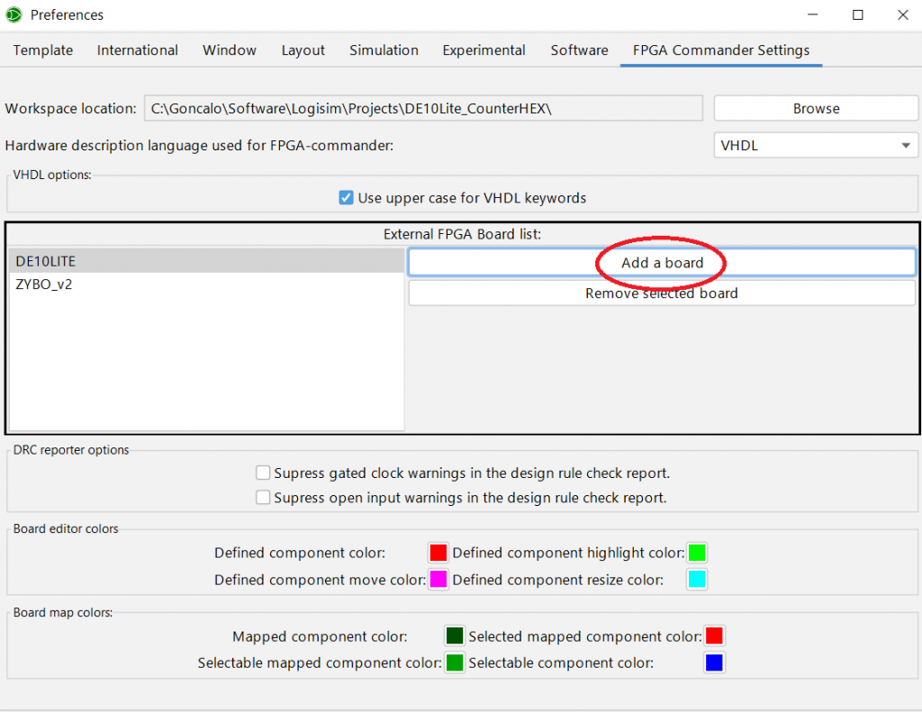
You should be able to see and select the new board under "Target board"