PCB Design Workshop
The goal with this workshop is to introduce students to the PCB design mind set, from capturing an idea (prototyping), design, simulation (whenever possible), layout, and manufacturing.
Required Software
KiCad 6 is an open source software suite for Electronic Design Automation (EDA). The programs handle Schematic Capture, and PCB Layout with Gerber output. The suite runs on Windows, Linux and macOS and is licensed under GNU GPL v3.
A good portion of the concepts covered in this workshop can be applied with other EDAs software (e.g. Altium, Eagle, easyEDA, DipTrace, etc). Some software can be more user friendly than others, but remember that the goal is to develop the mind set behind designing PCB's.
Other software used (not required)

Fusion 360 is a cloud-based 3D modeling, CAD, CAM, CAE, and PCB software platform for product design and manufacturing. The CAD portion of this software is used to generate front panels and board layouts. Any other CAD software can be used as long as it can handle DXF and STEP files.

Inkscape is a free and open-source vector graphics editor used to create vector images, primarily in Scalable Vector Graphics format. Other formats can be imported and exported. Inkscape can render primitive vector shapes and text. Inkscape is used for the aesthetics portion (silkscreen) of the PCB boards.
Modules
Quick Prototype
Develop an Arduino shield with off-the-shelf components.
(Example)
Introduction
- Introduction
- Project/Folder & Libraries structure
- KiCad main window overview
- Plugins and Content Manager
- Calculator
- Footprint and Symbol Editor
- Gerber Viewer
- Image Converter
- Schematic and PCB Editor
Schematic
- Schematic
- Page setup
- Place components
- Select footprint
- Place power components
- Connect components
- Add relevant text and sections
- Annotations
- Run ERC
PCB Layout
- PCB Layout
- Page setup
- Board Layers
- Update PCB components
- Components placement
- Physical constraints
- Silkscreen
- Export STEP file
PCB Routing
- PCB Routing
- Ground layer
- Trace thickness
- Run DRC
- Silkscreen update
Manufacturing
- Manufacturing
- Gerber files
- Order PCB online
Analog Design Example
Develop a simple Eurorack Module (2 input and 1 output analog mixer)
(Example)
Introduction
- Introduction
- Project description
- System requirements
- Components selection
- Schematic draft
Schematic
- Schematic
- Import schematic
- Manage symbol library
- Manage footprint library (PCB Layout)
Support Files
Libraries.zip
Eurorack_PowerConnectors.zip
EurorackMixer_incomplete.zip
PCB Layout
- PCB Layout
- Board layers
- Board layouts (Edge Cuts)
- Import DXF files
- Update PCB components
- Add 3D models
- Add components on bottom layers
- Place components
- Silkscreen
- Export STEP file
PCB Routing
- PCB Routing
- Ground layer
- Trace thickness
- Run DRC
- Silkscreen update
Manufacturing
- Manufacturing
- Gerber files
- BOM and CPL files
- Order PCB online
Other PCB Examples
Learn by reverse engineering other boards.
Microprocessor Designs
Phil’s Lab Tutorials
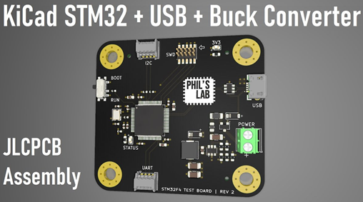
- KiCad STM32 + USB + Buck Converter (YouTube Link)
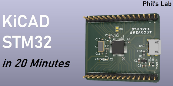
- KiCad STM32 in 20 minutes (YouTube Link)
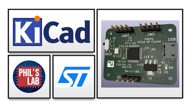
- Udemy course (KiCad STM32) (YouTube Link)
Radio Frequency Designs
Mixed Signal Designs

FPGA Designs
Power Supply Designs
- Soon
Text and Graphics
Soon...
Simulations
Soon...
Other Resources