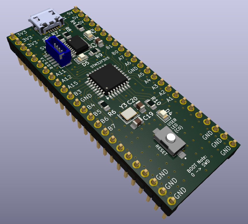
STM32F303 With Teensy Layout
STM32F303K676 with Teensy Layout
✔️ Introduction
✔️ Design Experience
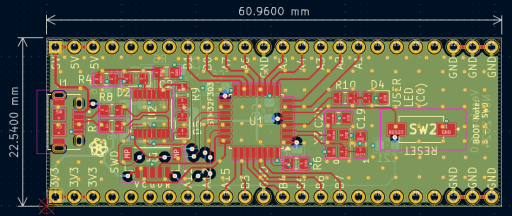
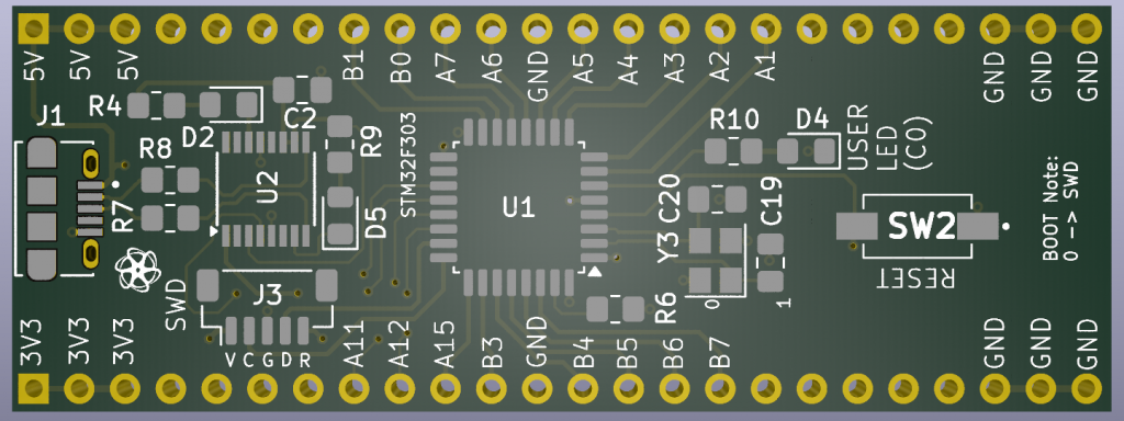
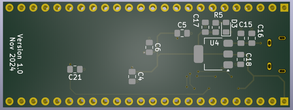
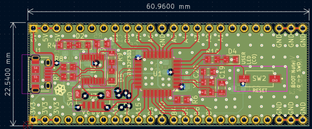
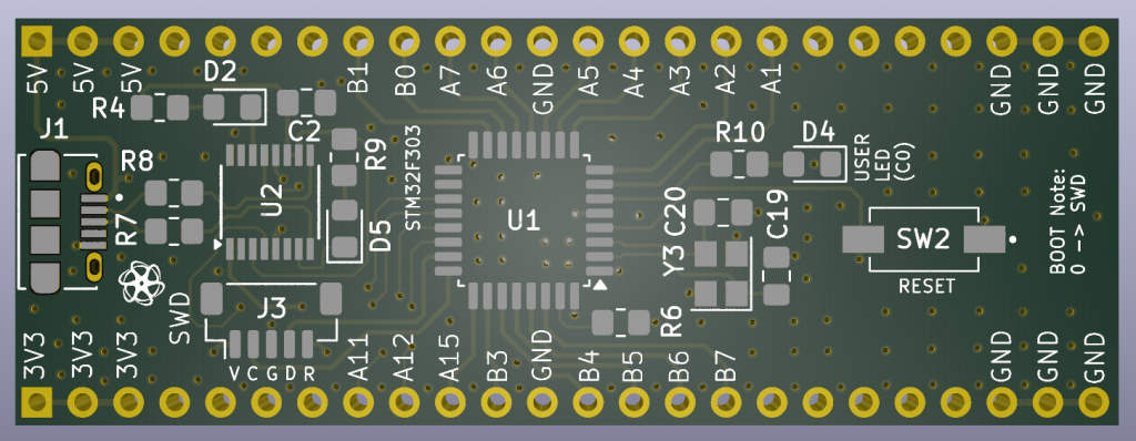
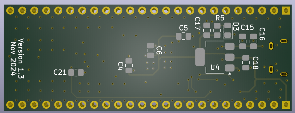
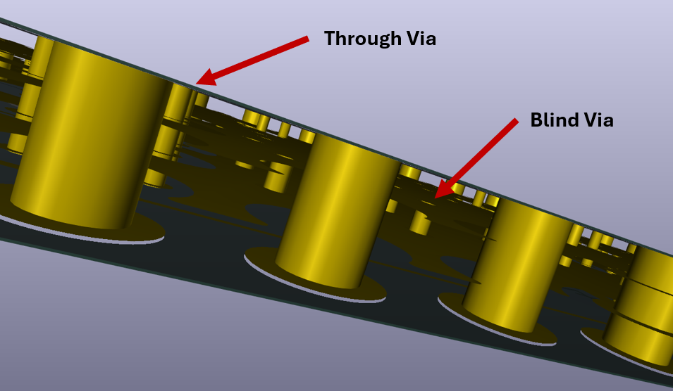
This was an interesting project mainly because I got to experience the design of a 4 layer board with blind vias. However, due to the high cost of manufacturing a PCB board with blind vias, I changed the design to use only through vias.
✔️ Assemble Stage
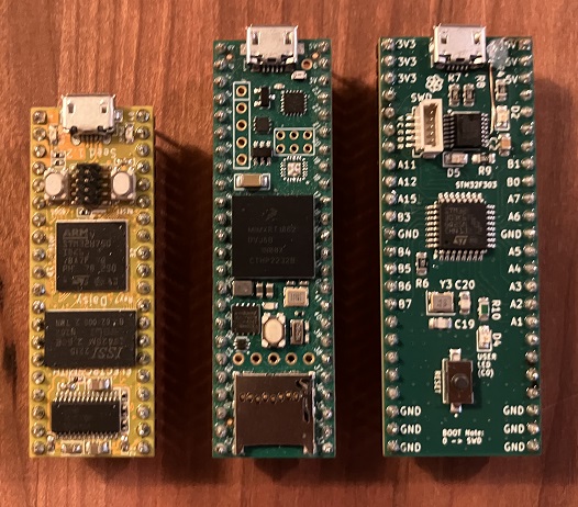
The boards were manufactured and assembled by PCBWay. As always a wonderful job.
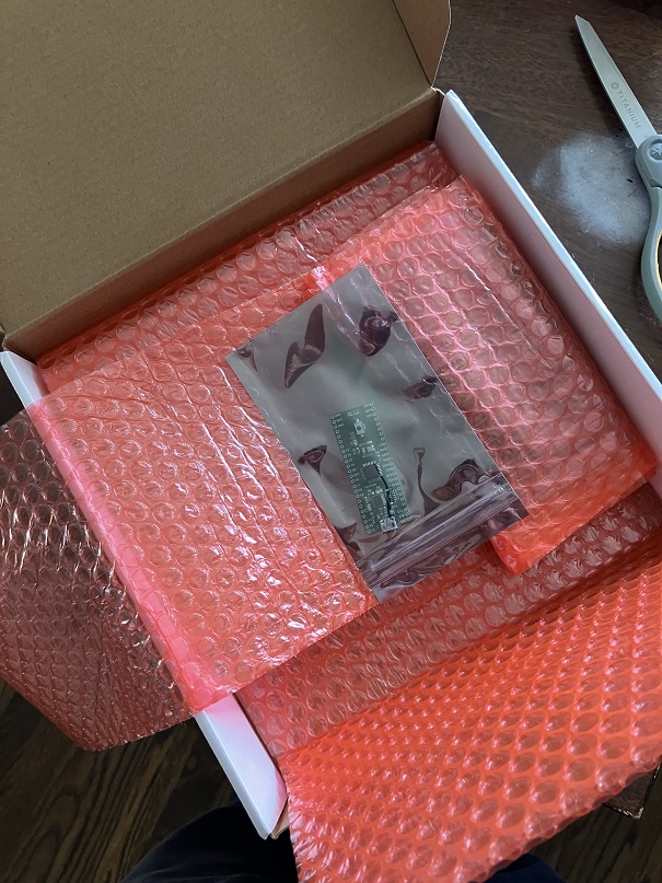
One of the aspects I appreciate most about PCBWay’s assembly service is the consistent communication throughout the entire process, ensuring everything proceeds smoothly. For instance, after submitting the component list, PCBWay promptly confirmed receipt of all the requested components. If any files are missing, they notify me via email and respond quickly. During the assembly, they verify that all components are correctly soldered.
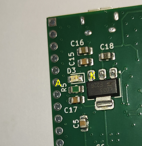
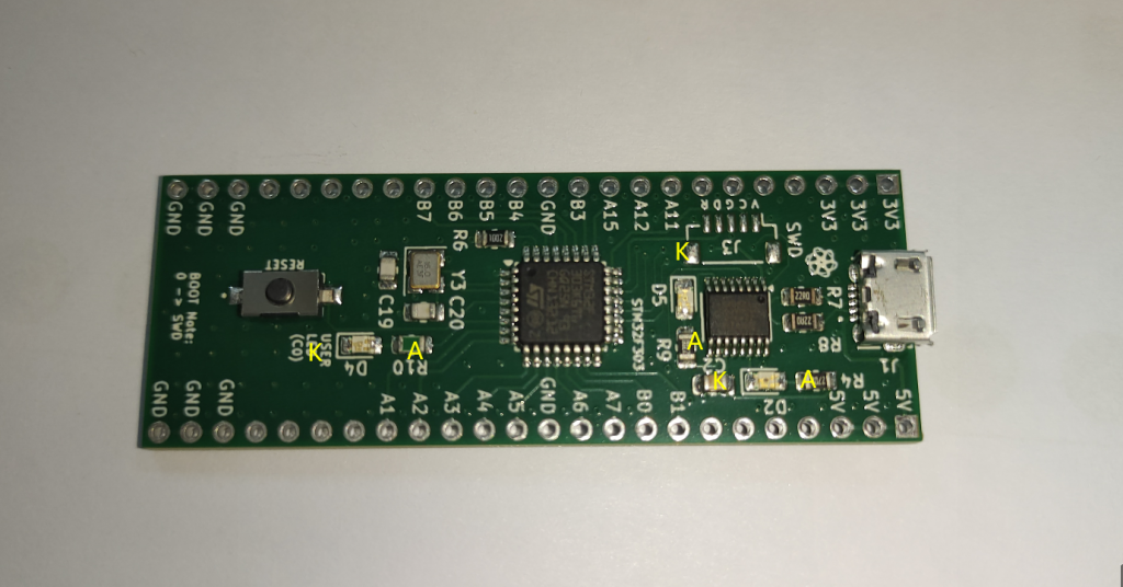
Finally, once the board is ready for shipment, I receive a notification that it is on its way.
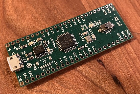
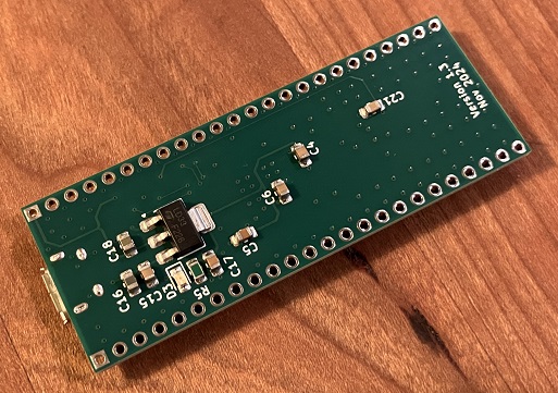
Assembling a board can be a time-consuming process, but the professional behavior and prompt communication from PCBWay instill confidence in their assembly service, making it a reliable choice for future projects with tight deadlines.
The JST connector was soldered onto the board manually after it was received. This was a deliberate design choice, as I could not source the part in time before submitting the files for production.
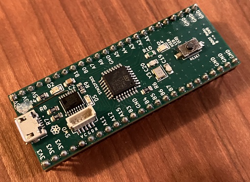
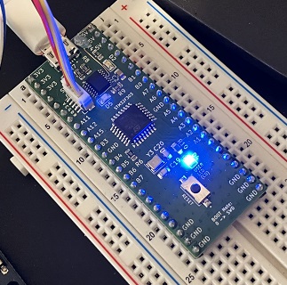
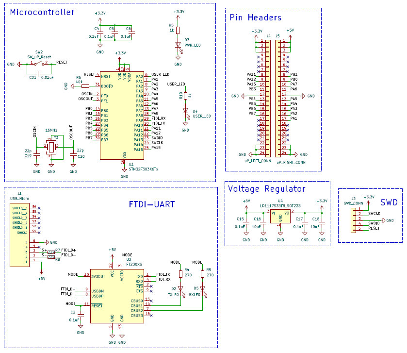
Quick Note: At this stage I reuse a lot of schematics from previous designs since I know that everything is going to work properly. However, for this design I didn’t pay attention that the power pin for the FTDI chip should have been connected to the +5V label and instead I left it with the name assigned from the previous project (Vusb). To fix that issue, I needed to solder a wire to power the FTDI chip to +5V. All designs and files from the PCB design section were fixed accordingly.
✔️ Programmer/Debugger Adapter
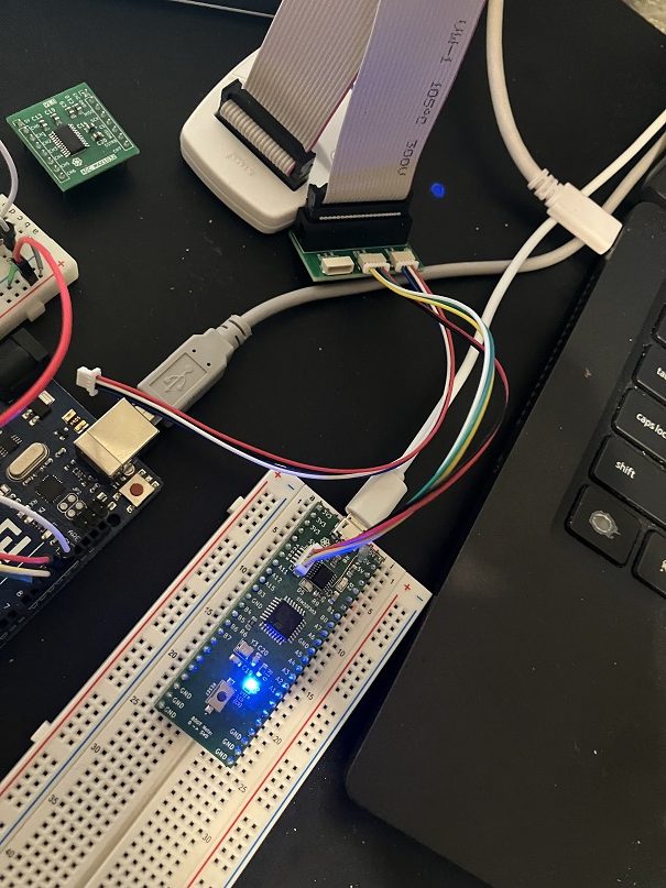
To program the board I am using the ST-Link/V2 that has a 20-pin header connector that exposes all the pins needed for full JTAG and SWD support.
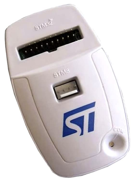
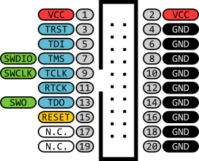
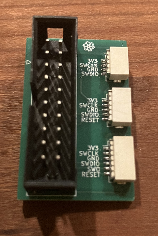
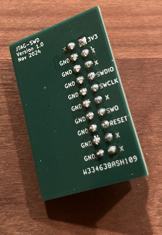
However, the STM32C011J board has a 1mm 4-pin JST connector. With that in mind I created an interface board to connect the SWD pins from the debugger to the STM32C011J. This interface board allows to connect 3 different types of SWD configurations:
- 3V3 / SWCLK / GND / SWDIO (4-pin JST)
- 3V3 / SWCLK / GND / SWDIO / RESET (5-pin JST)
- 3V3 / SWCLK / GND / SWDIO / SWO / RESET (6-pin JST)
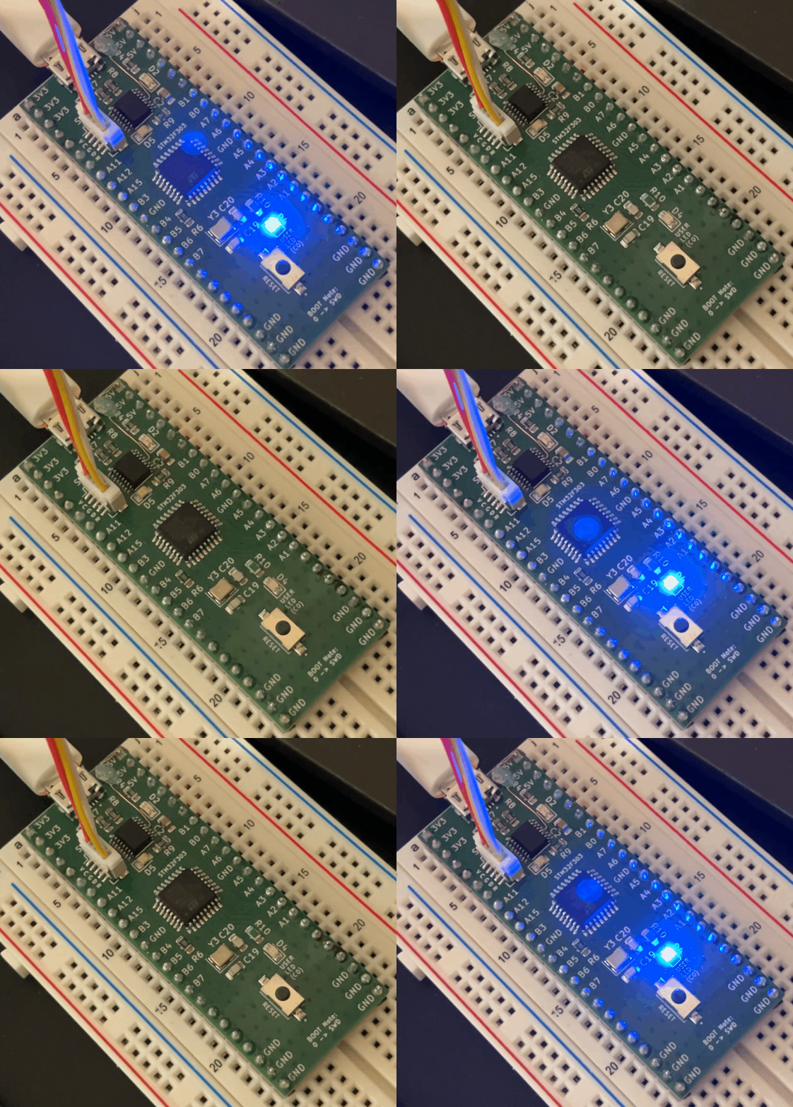
✔️ Blink LED Test
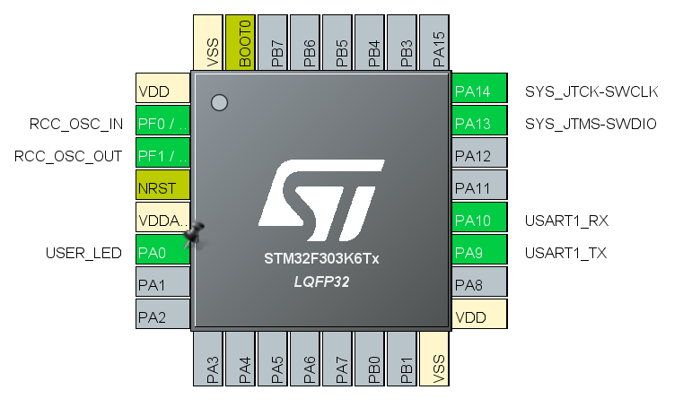
The PCB board has a user led on pin PA0.

✔️ UART Test
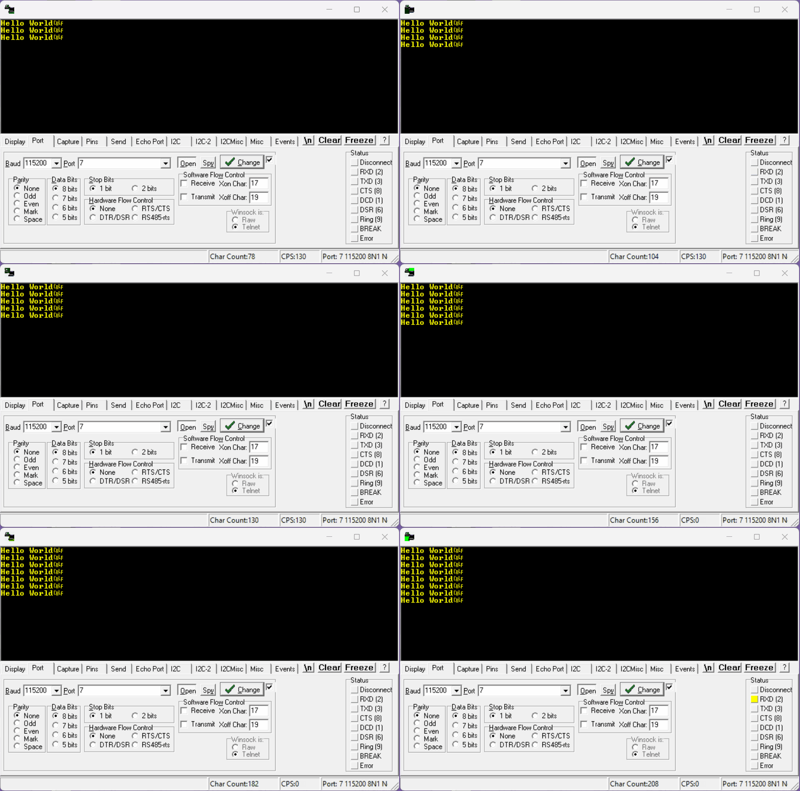
The UART was also tested by printing “Hello World” at the same speed as the LED is blinking.
✔️ GitHub Repository
✔️ References
- NA
Sponsor

