Toggle LED
Let's start by doing a simple project that toggles an LED so we can get familiar with the IDE and the sequence of steps required to program an FPGA.
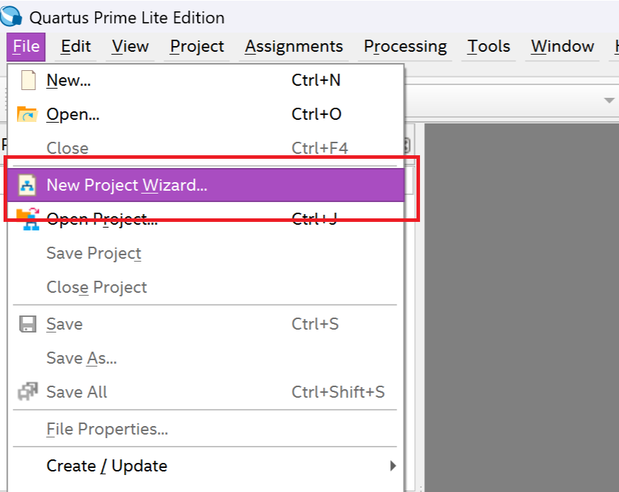
Step 1 - Create a New Project
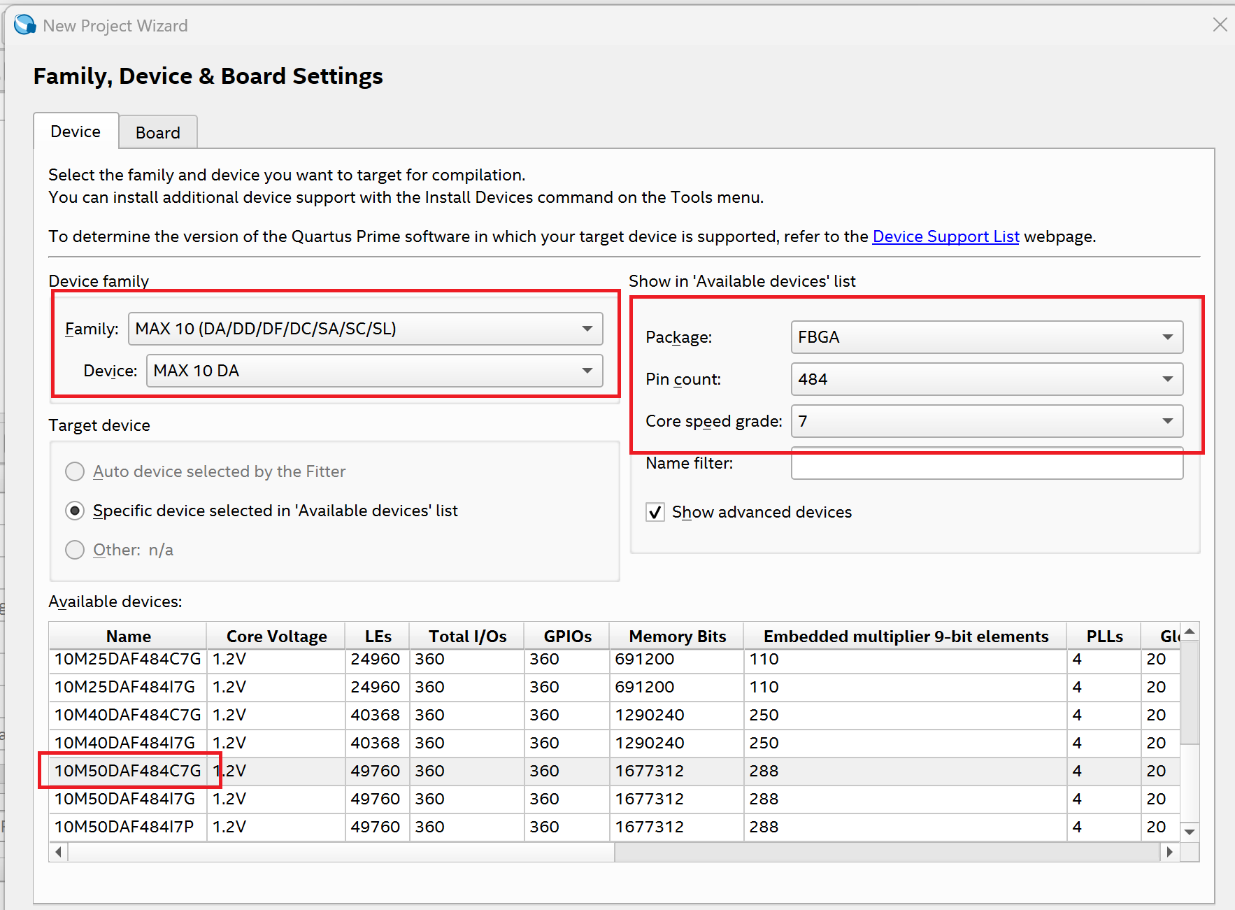
The DE10-Lite development board uses the Intel (formerly Altera) MAX 10 FPGA, specifically the 10M50DAF484C7G device.
Key details about this FPGA:
- Family: Intel MAX 10
- Logic Elements (LEs): ~50,000
- Package: 484-pin FBGA
- On-chip Flash memory: Yes (configuration and user storage)
- Embedded memory: ~1.6 Mbits
- ADC (Analog-to-Digital Converter): Dual 12-bit, 1 MSPS ADCs built in
Go to file and create a new project and let the wizard help you.
Note
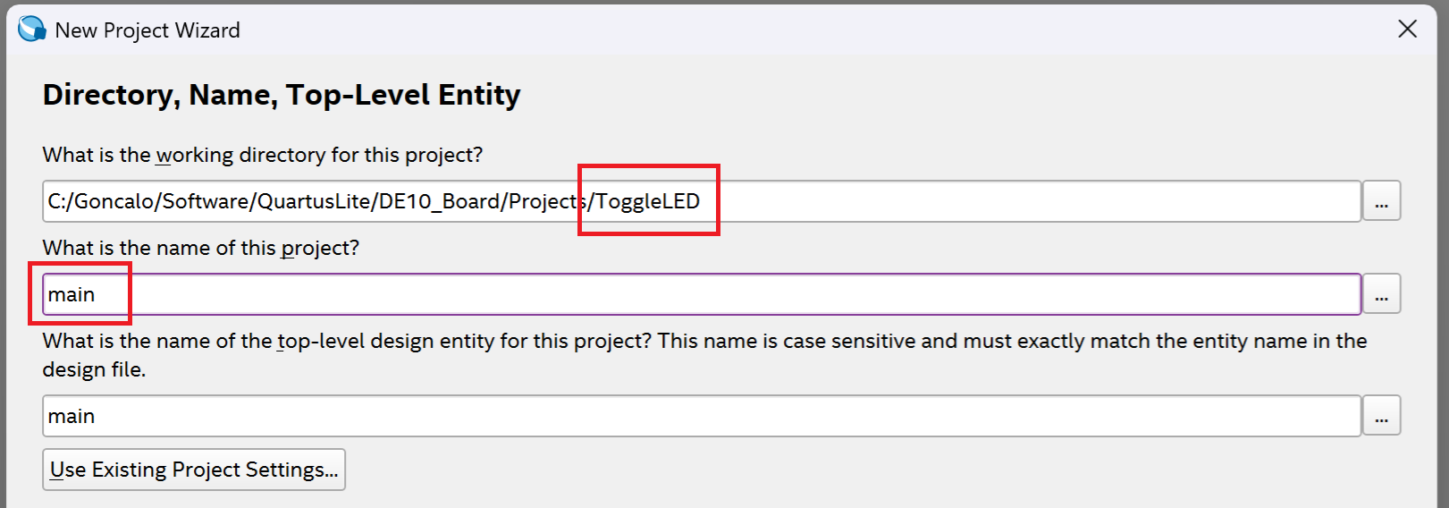
Make sure that you create a folder with the name of the project before you do the next step.
For projects developed in Quartus, I consistently name the project "main." This becomes especially useful for larger projects, where identifying the top-level file is important. Using "main" makes it easier to quickly locate it.
Press next, choose empty project and don't add any files.
Now it is time to choose the FPGA family that we are going to use. Follow the image below. After that press next and finish the setup.
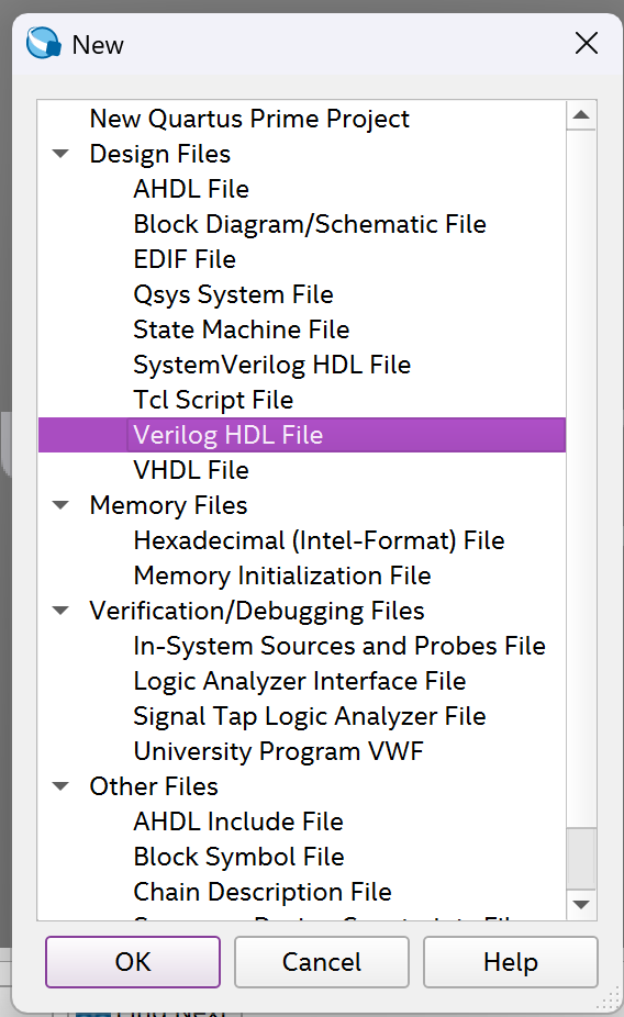
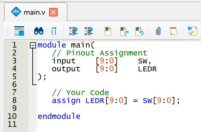
Step 2 - Create Verilog File
Go to "File->New" and create a new Verilog file.
For now, write the code below and save the file with the name "main.v".
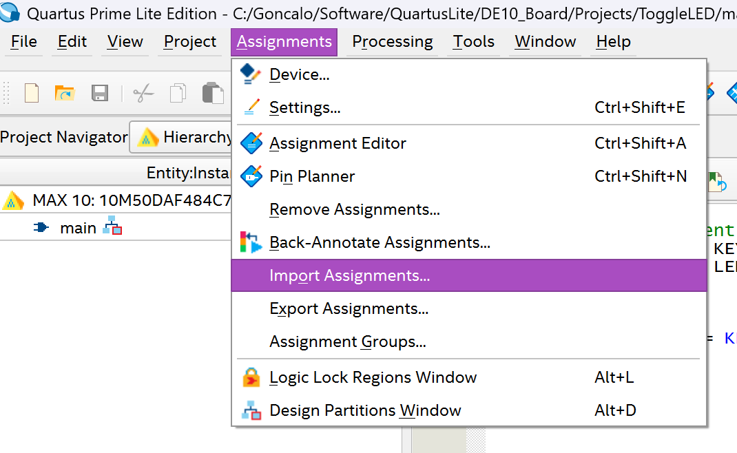
Step 3 - Pinout Mapping
Now it is time to assign the inputs and outputs of the "main.v" file to real I/Os on the FPGA. We can choose to do this manually by using the Assignment Editor or Pin Planner, but it is easier to import all the pinouts at once from a "qsf" file.
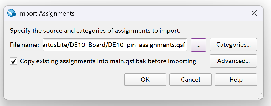
Go to Assignments and select "Import Assignments..."
For the file name, put the path to the folder where you have the "DE10_pin_assignments.qsf".
Note
You can download that file from the links under References.
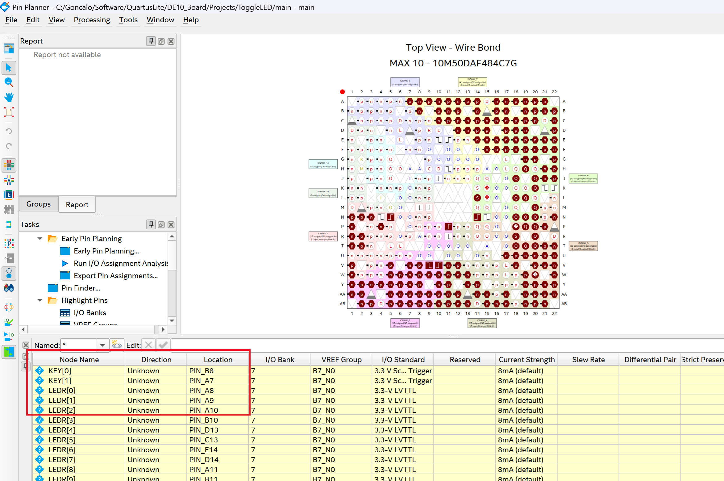
Press ok and check the pin planner under "Assignments -> pin planner". Check if the names of your input and outputs variables are the same as the "Node Name" names.
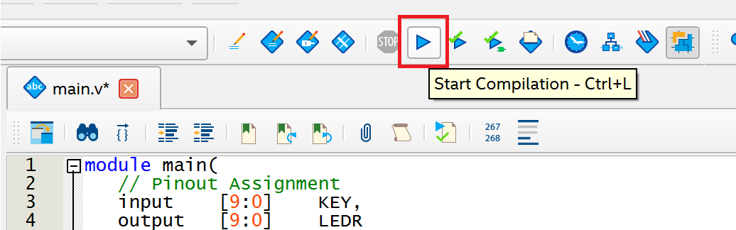
Step 4 - Start Synthesis
Press the blue play button to start "compilation".
Note
Compilation for Quartus IDE is a catch-all for the whole process of synthesis -> fitting -> bitstream generation.
- Synthesis: Converts HDL code into a gate-level netlist that represents the logical design.
- Fitting (Place-and-Route): Maps that netlist onto the physical FPGA resources (logic elements, DSPs, I/O pins, etc.).
- Bitstream Generation: Produces the configuration file (.sof, .pof, etc.) that is loaded into the FPGA
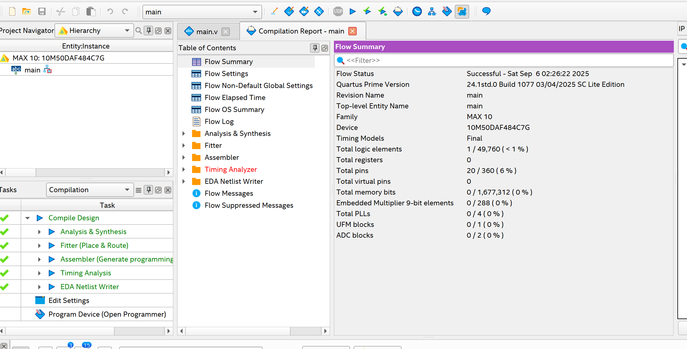
After compilation is done and if you don't have errors in your HDL code, you should see a "Flow Summary" window with results of resources used.
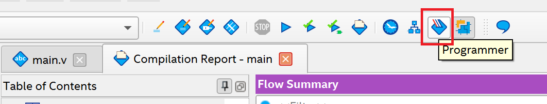
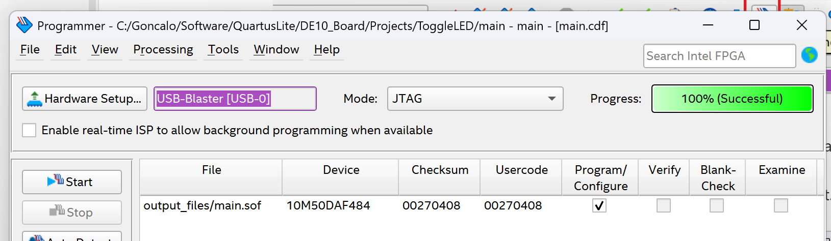
Step 5 - Programming
Last step is to program the FPGA with the bitstream file generated in the previous step. Select the programmer button.
Make sure that the FPGA is connected to the computer and the JTAG drivers are installed properly.
You should see under File the "main.sof" file and press start if all looks correct.
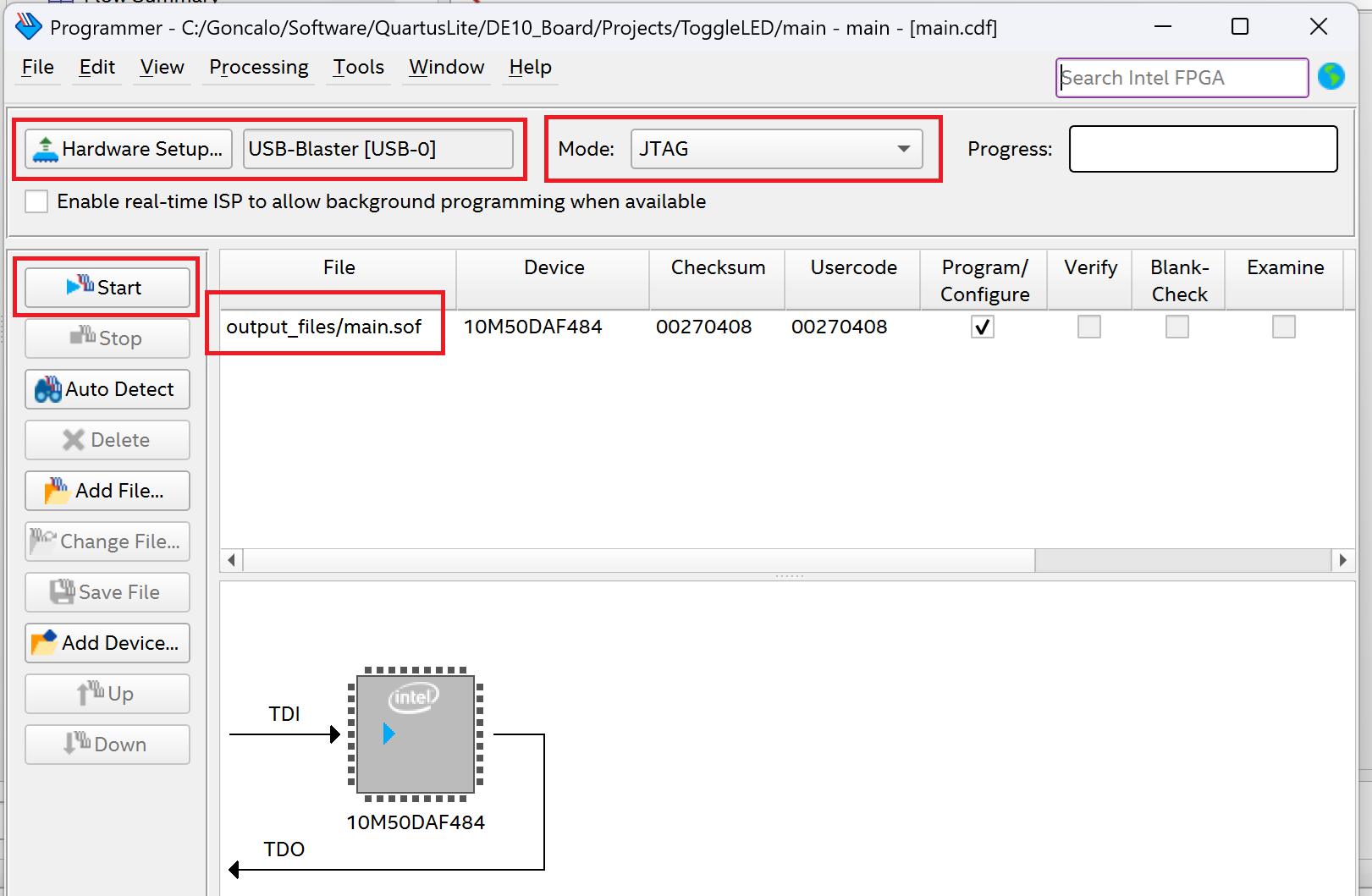
If all goes well, you will see a 100% (Successful) message on the screen.
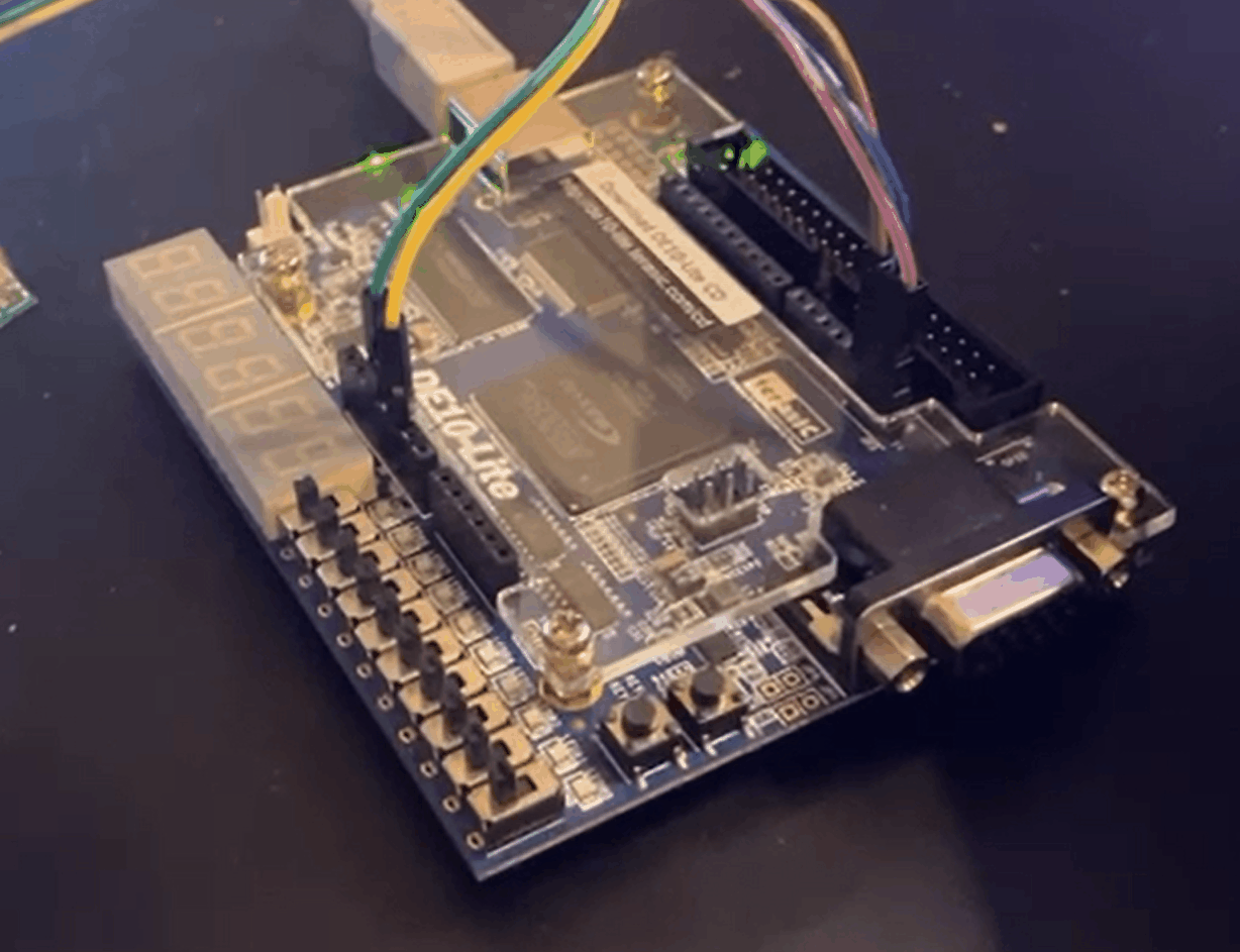
You should be able to toggle the buttons and the LEDs should turn on and off accordingly.
References
- DE10-Lite Official Website Documentation
- DE10-Lite Online Manual
- DE10_pin_assignments.qsf download